Journals > > Topics > Plasmonics and Metamaterials
Plasmonics and Metamaterials|8 Article(s)
Transparently curved metamaterial with broadband millimeter wave absorption
Cheng Zhang, Jin Yang, Wenkang Cao, Wei Yuan, Junchen Ke, Liuxi Yang, Qiang Cheng, and Tiejun Cui
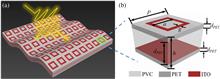
We present a conformal metamaterial with simultaneous optical transparency and broadband millimeter-wave absorption for a curved surface. By tailoring the reflection response of meta-atoms at oblique angles, it is possible to achieve excellent absorption performance from 26.5 to 40.0 GHz within a wide angular range from 0° to 60° for transverse-electric and transverse-magnetic waves. In the meantime, by employing transparent substrates, including polyvinyl chloride and polyethylene terephthalate, good optical transmittance (80.1%) and flexibility are obtained simultaneously. The reflectivity of a curved metallic surface coated with the proposed curved metamaterial is simulated and measured experimentally. Both results demonstrate excellent absorption performance of the metamaterial, which is highly favored for practical applications. We present a conformal metamaterial with simultaneous optical transparency and broadband millimeter-wave absorption for a curved surface. By tailoring the reflection response of meta-atoms at oblique angles, it is possible to achieve excellent absorption performance from 26.5 to 40.0 GHz within a wide angular range from 0° to 60° for transverse-electric and transverse-magnetic waves. In the meantime, by employing transparent substrates, including polyvinyl chloride and polyethylene terephthalate, good optical transmittance (80.1%) and flexibility are obtained simultaneously. The reflectivity of a curved metallic surface coated with the proposed curved metamaterial is simulated and measured experimentally. Both results demonstrate excellent absorption performance of the metamaterial, which is highly favored for practical applications.
Photonics Research
- Publication Date: Apr. 11, 2019
- Vol. 7, Issue 4, 04000478 (2019)


Experimental demonstration of ultra-large-scale terahertz all-dielectric metamaterials
Ke Bi, Daquan Yang, Jia Chen, Qingmin Wang, Hongya Wu, Chuwen Lan, and Yuping Yang
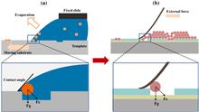
All-dielectric metamaterials have emerged as a promising platform for low-loss and highly efficient terahertz devices. However, existing fabrication methods have difficulty in achieving a good balance between precision and cost. Here, inspired by the nano-template-assisted self-assembly method, we develop a micro-template-assisted self-assembly (MTAS) method to prepare large-scale, high-precision, and flexible ceramic microsphere all-dielectric metamaterials with an area exceeding 900 cm×900 cm. Free from organic solvents, vacuum, and complex equipment, the MTAS method ensures low-cost and environmentally friendly fabrication. The ceramic microsphere resonators can be readily assembled into nearly arbitrary arrangements and complex aggregates, such as dimers, trimers, quadrumers, and chains. Finally, using the heat-shrinkable substrate and dipole coupling effect, a broadband reflector with a bandwidth of 0.15 THz and a reflection of up to 95% is demonstrated. This work provides a versatile and powerful platform for terahertz all-dielectric metamaterials, with potential to be applied in a wide variety of high-efficiency terahertz devices. All-dielectric metamaterials have emerged as a promising platform for low-loss and highly efficient terahertz devices. However, existing fabrication methods have difficulty in achieving a good balance between precision and cost. Here, inspired by the nano-template-assisted self-assembly method, we develop a micro-template-assisted self-assembly (MTAS) method to prepare large-scale, high-precision, and flexible ceramic microsphere all-dielectric metamaterials with an area exceeding 900 cm×900 cm. Free from organic solvents, vacuum, and complex equipment, the MTAS method ensures low-cost and environmentally friendly fabrication. The ceramic microsphere resonators can be readily assembled into nearly arbitrary arrangements and complex aggregates, such as dimers, trimers, quadrumers, and chains. Finally, using the heat-shrinkable substrate and dipole coupling effect, a broadband reflector with a bandwidth of 0.15 THz and a reflection of up to 95% is demonstrated. This work provides a versatile and powerful platform for terahertz all-dielectric metamaterials, with potential to be applied in a wide variety of high-efficiency terahertz devices.
Photonics Research
- Publication Date: Apr. 11, 2019
- Vol. 7, Issue 4, 04000457 (2019)
Efficient spectrum prediction and inverse design for plasmonic waveguide systems based on artificial neural networks
Tian Zhang, Jia Wang, Qi Liu, Jinzan Zhou, Jian Dai, Xu Han, Yue Zhou, and Kun Xu
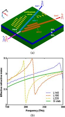
In this paper, we propose a novel approach to achieve spectrum prediction, parameter fitting, inverse design, and performance optimization for the plasmonic waveguide-coupled with cavities structure (PWCCS) based on artificial neural networks (ANNs). The Fano resonance and plasmon-induced transparency effect originated from the PWCCS have been selected as illustrations to verify the effectiveness of ANNs. We use the genetic algorithm to design the network architecture and select the hyperparameters for ANNs. Once ANNs are trained by using a small sampling of the data generated by the Monte Carlo method, the transmission spectra predicted by the ANNs are quite approximate to the simulated results. The physical mechanisms behind the phenomena are discussed theoretically, and the uncertain parameters in the theoretical models are fitted by utilizing the trained ANNs. More importantly, our results demonstrate that this model-driven method not only realizes the inverse design of the PWCCS with high precision but also optimizes some critical performance metrics for the transmission spectrum. Compared with previous works, we construct a novel model-driven analysis method for the PWCCS that is expected to have significant applications in the device design, performance optimization, variability analysis, defect detection, theoretical modeling, optical interconnects, and so on. In this paper, we propose a novel approach to achieve spectrum prediction, parameter fitting, inverse design, and performance optimization for the plasmonic waveguide-coupled with cavities structure (PWCCS) based on artificial neural networks (ANNs). The Fano resonance and plasmon-induced transparency effect originated from the PWCCS have been selected as illustrations to verify the effectiveness of ANNs. We use the genetic algorithm to design the network architecture and select the hyperparameters for ANNs. Once ANNs are trained by using a small sampling of the data generated by the Monte Carlo method, the transmission spectra predicted by the ANNs are quite approximate to the simulated results. The physical mechanisms behind the phenomena are discussed theoretically, and the uncertain parameters in the theoretical models are fitted by utilizing the trained ANNs. More importantly, our results demonstrate that this model-driven method not only realizes the inverse design of the PWCCS with high precision but also optimizes some critical performance metrics for the transmission spectrum. Compared with previous works, we construct a novel model-driven analysis method for the PWCCS that is expected to have significant applications in the device design, performance optimization, variability analysis, defect detection, theoretical modeling, optical interconnects, and so on.
Photonics Research
- Publication Date: Mar. 01, 2019
- Vol. 7, Issue 3, 03000368 (2019)
Ultra-compact on-chip metaline-based 1.3/1.6 μm wavelength demultiplexer
Yulong Fan, Xavier Le Roux, Anatole Lupu, and André de Lustrac
In this paper, we report an experimental demonstration of enabling technology exploiting resonant properties of plasmonic nanoparticles, for the realization of wavelength-sensitive ultra-minituarized (4 μm×4 μm) optical metadevices. To this end, the example of a 1.3/1.6 μm wavelength demultiplexer is considered. Its technological implementation is based on the integration of gold cut-wire-based metalines on the top of a silicon-on-insulator waveguide. The plasmonic metalines modify locally the effective index of the Si waveguide and thus allow for the implementation of wavelength-dependent optical pathways. The 1.3/1.6 μm wavelength separation with extinction ratio between two demultiplexers’ channels reaching up to 20 dB is experimentally demonstrated. The considered approach, which can be readily adapted to different types of material planar lightwave circuit platforms and nanoresonators, is suited for the implementation of a generic family of wavelength-sensitive guided-wave optical metadevices. In this paper, we report an experimental demonstration of enabling technology exploiting resonant properties of plasmonic nanoparticles, for the realization of wavelength-sensitive ultra-minituarized (4 μm×4 μm) optical metadevices. To this end, the example of a 1.3/1.6 μm wavelength demultiplexer is considered. Its technological implementation is based on the integration of gold cut-wire-based metalines on the top of a silicon-on-insulator waveguide. The plasmonic metalines modify locally the effective index of the Si waveguide and thus allow for the implementation of wavelength-dependent optical pathways. The 1.3/1.6 μm wavelength separation with extinction ratio between two demultiplexers’ channels reaching up to 20 dB is experimentally demonstrated. The considered approach, which can be readily adapted to different types of material planar lightwave circuit platforms and nanoresonators, is suited for the implementation of a generic family of wavelength-sensitive guided-wave optical metadevices.
Photonics Research
- Publication Date: Feb. 28, 2019
- Vol. 7, Issue 3, 03000359 (2019)
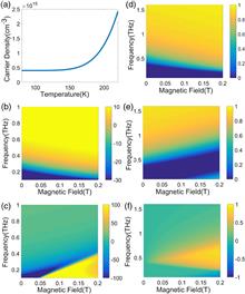
Tunable magneto-optical polarization device for terahertz waves based on InSb and its plasmonic structure
Qianyi Mu, Fei Fan, Sai Chen, Shitong Xu, Chuanzhong Xiong, Xin Zhang, Xianghui Wang, and Shengjiang Chang
The nonreciprocal circular dichroism and Faraday rotation effect for terahertz (THz) waves in longitudinally magnetized InSb were investigated by theoretical and experimental studies in the THz regime, which indicated its ability for a THz circularly polarized isolator, THz circular polarizer, tunable polarization converter, and polarization modulator by manipulation of different magnetic fields. Furthermore, we demonstrated the InSb plasmonics based on its magneto-optical effects combined with artificial microstructure. We found the magneto-optical enhancement mechanisms in this magneto-plasmonic structure, achieving broadband near-perfect orthogonal linear polarization conversion modulated by the weak magnetic field in an experiment with an extinction ratio of 33 dB. Moreover, the magneto-optical modulation with an amplitude modulation depth of 95.8% can be achieved by this device under a weak magnetic field of 150 mT. InSb and its magneto-plasmonic device have broad potential for a THz isolator, magneto-optical modulator, and polarization convertor in THz application systems. The nonreciprocal circular dichroism and Faraday rotation effect for terahertz (THz) waves in longitudinally magnetized InSb were investigated by theoretical and experimental studies in the THz regime, which indicated its ability for a THz circularly polarized isolator, THz circular polarizer, tunable polarization converter, and polarization modulator by manipulation of different magnetic fields. Furthermore, we demonstrated the InSb plasmonics based on its magneto-optical effects combined with artificial microstructure. We found the magneto-optical enhancement mechanisms in this magneto-plasmonic structure, achieving broadband near-perfect orthogonal linear polarization conversion modulated by the weak magnetic field in an experiment with an extinction ratio of 33 dB. Moreover, the magneto-optical modulation with an amplitude modulation depth of 95.8% can be achieved by this device under a weak magnetic field of 150 mT. InSb and its magneto-plasmonic device have broad potential for a THz isolator, magneto-optical modulator, and polarization convertor in THz application systems.
Photonics Research
- Publication Date: Feb. 26, 2019
- Vol. 7, Issue 3, 03000325 (2019)

All-angle optical switch based on the zero reflection effect of graphene–dielectric hyperbolic metamaterials
Wenyao Liang, Zheng Li, Yu Wang, Wuhe Chen, and Zhiyuan Li
We have studied a switchable hyperbolic metamaterial composed of a graphene–dielectric periodic structure. By tuning the chemical potential of all graphene sheets simultaneously, the isofrequency curve can switch between an ellipse and a hyperbola conveniently. In particular, a special hyperbolic isofrequency curve with its asymptote perpendicular to the interface is obtained and used to realize the zero reflection effect. Furthermore, a zero-reflection-based optical switch working in the terahertz spectrum is demonstrated. Its bandwidth can be efficiently adjusted by geometric parameters such as permittivity and period. Such an optical switch possesses the merits of low loss, high transmittance contrast, high response speed, compact size, high tolerance of chemical potential, and having all incident angles (0°–90°) simultaneously. Such an optical switch holds great potential in many fields, such as data storage, beam steering, and integrated photonic circuits. We have studied a switchable hyperbolic metamaterial composed of a graphene–dielectric periodic structure. By tuning the chemical potential of all graphene sheets simultaneously, the isofrequency curve can switch between an ellipse and a hyperbola conveniently. In particular, a special hyperbolic isofrequency curve with its asymptote perpendicular to the interface is obtained and used to realize the zero reflection effect. Furthermore, a zero-reflection-based optical switch working in the terahertz spectrum is demonstrated. Its bandwidth can be efficiently adjusted by geometric parameters such as permittivity and period. Such an optical switch possesses the merits of low loss, high transmittance contrast, high response speed, compact size, high tolerance of chemical potential, and having all incident angles (0°–90°) simultaneously. Such an optical switch holds great potential in many fields, such as data storage, beam steering, and integrated photonic circuits.
Photonics Research
- Publication Date: Feb. 25, 2019
- Vol. 7, Issue 3, 03000318 (2019)
Silica nanocone array as a template for fabricating a plasmon induced hot electron photodetector|On the Cover
Zhiqiang Yang, Kang Du, Fanfan Lu, Yang Pang, Shijia Hua, Xuetao Gan, Wending Zhang, Soo Jin Chua, and Ting Mei
Plasmon induced hot electrons have attracted a great deal of interest as a novel route for photodetection and light-energy harvesting. Herein, we report a hot electron photodetector in which a large array of nanocones deposited sequentially with aluminum, titanium dioxide, and gold films can be integrated functionally with nanophotonics and microelectronics. The device exhibits a strong photoelectric response at around 620 nm with a responsivity of 180 μA/W under short-circuit conditions with a significant increase under 1 V reverse bias to 360 μA/W. The increase in responsivity and a red shift in the peak value with increasing bias voltage indicate that the bias causes an increase in the hot electron tunneling effect. Our approach will be advantageous for the implementation of the proposed architecture on a vast variety of integrated optoelectronic devices. Plasmon induced hot electrons have attracted a great deal of interest as a novel route for photodetection and light-energy harvesting. Herein, we report a hot electron photodetector in which a large array of nanocones deposited sequentially with aluminum, titanium dioxide, and gold films can be integrated functionally with nanophotonics and microelectronics. The device exhibits a strong photoelectric response at around 620 nm with a responsivity of 180 μA/W under short-circuit conditions with a significant increase under 1 V reverse bias to 360 μA/W. The increase in responsivity and a red shift in the peak value with increasing bias voltage indicate that the bias causes an increase in the hot electron tunneling effect. Our approach will be advantageous for the implementation of the proposed architecture on a vast variety of integrated optoelectronic devices.
Photonics Research
- Publication Date: Feb. 19, 2019
- Vol. 7, Issue 3, 03000294 (2019)
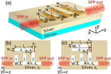
Subwavelength negative-index waveguiding enabled by coupled spoof magnetic localized surface plasmons
Zhen Liao, Guo Qing Luo, Ben Geng Cai, Bai Cao Pan, and Wen Hui Cao
Magnetic localized surface plasmon modes are supported on metallic spiral structures. Coupling mechanisms for these metamaterial resonators, which are the joint action of magnetic and electric coupling, are studied. Based on the strong coupling, spoof magnetic plasmon modes propagating in the backward direction are proposed along a chain of subwavelength resonators. The theoretical analysis, numerical simulations, and experiments are in good agreement. The proposed novel route for achieving negative-index waveguiding has potential applications in integrated devices and circuits. Magnetic localized surface plasmon modes are supported on metallic spiral structures. Coupling mechanisms for these metamaterial resonators, which are the joint action of magnetic and electric coupling, are studied. Based on the strong coupling, spoof magnetic plasmon modes propagating in the backward direction are proposed along a chain of subwavelength resonators. The theoretical analysis, numerical simulations, and experiments are in good agreement. The proposed novel route for achieving negative-index waveguiding has potential applications in integrated devices and circuits.
Photonics Research
- Publication Date: Feb. 12, 2019
- Vol. 7, Issue 3, 03000274 (2019)
Topics
© Copyright 2018-2021 | Chinese Laser Press. All Rights Reserved 沪ICP备15018463号-20